Knowledge

EDX Analysis with a Scanning Electron Microscope (SEM): How Does it Work?

Electron – matter interaction

The electron beam-matter interaction generates a variety of signals that carry different information about the sample (Figure1). For example, backscattered electrons produce images with contrast that carries information on the differences in atomic number; secondary electrons give topographic information (you can read more about it here); cathodoluminescence can give information on the electronic structure and the chemical composition of materials; and transmitted electrons can describe the sample’s inner structure and crystallography. Another type of signal that is widely used in SEMs is X-rays.


1-electron-matter-interaction.png

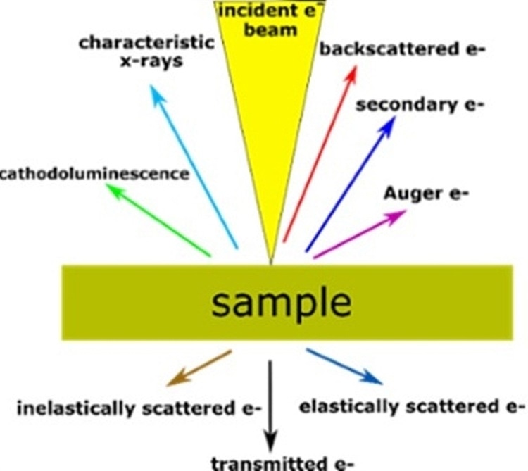
Figure 1. Illustration of the electron-matter interaction depicting its different products.
 

EDX analysis in SEM: the principle explained

Every atom has a unique number of electrons that reside under normal conditions in specific positions, as you can see in Figure 2. These positions belong to certain shells, which have different, discrete energies.

The generation of the X-rays in a SEM is a two-step process. In the first step, the electron beam hits the sample and transfers part of its energy to the atoms of the sample. This energy can be used by the electrons of the atoms to “jump” to an energy shell with higher energy or be knocked-off from the atom. If such a transition occurs, the electron leaves behind a hole. Holes have a positive charge and, in the second step of the process, attract the negatively-charged electrons from higher-energy shells. When an electron from such a higher-energy shell fills the hole of the lower-energy shell, the energy difference of this transition can be released in the form of an X-ray.

This X-ray has energy which is characteristic of the energy difference between these two shells. It depends on the atomic number, which is a unique property of every element. In this way, X-rays are a “fingerprint” of each element and can be used to identify the type of elements that exist in a sample.


EDX analysis with SEM

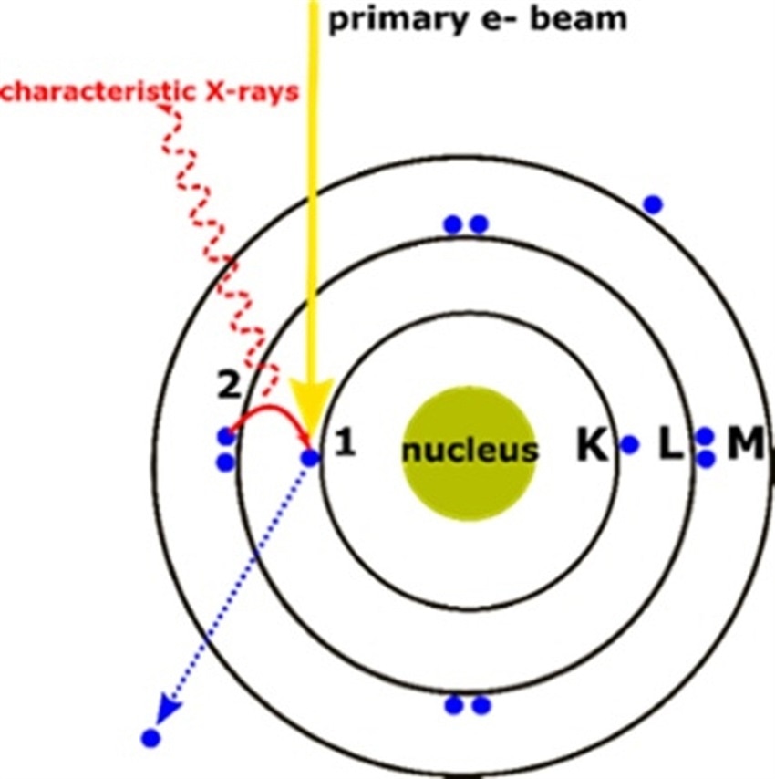
Figure 2. X-ray generation process. (1) The energy transferred to the atomic electron knocks it off leaving behind a hole, (2) its position is filled by another electron from a higher energy shell and the characteristic X-ray is released.
 

EDX material analysis: how X-ray detection works

Unlike BSE, SE and TE, X-rays are electromagnetic radiation, just like light, and consist of photons. To detect them, the latest systems use the so-called silicon-drift detectors (SDDs). These are superior to the conventional Si(Li) detectors due to higher count rates, better resolution, and faster analytical capabilitiesThese detectors are placed under an angle, very close to the sample, and have the ability to measure the energy of the incoming photons that belong to the X-rays. The higher the solid angle between the detector and the sample, the higher the X-rays’ detection probability, and therefore the likelihood of acquiring the best results.


EDX analysis with scanning electron microscope

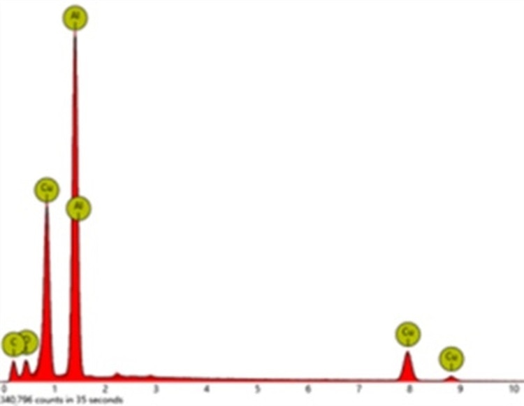
Figure 3. Typical EDX spectrum. Y-axis depicts the number of counts and x-axis the energy of the X-rays. The position of the peaks leads to the identification of the elements and the peak height helps in the quantification of each element’s concentration in the sample.
 

The data that is generated by EDX analysis consists of spectra with peaks corresponding to all the different elements that are present in the sample. You can see an example of this in Figure 3. Every element has characteristic peaks of unique energy, all extensively documented.

Furthermore, EDX can be used for qualitative (the type of elements) as well as quantitative (the percentage of the concentration of each element of the sample) analysis. In most SEMs, dedicated software enables auto-identification of the peaks and calculation of the atomic percentage of each element that is detected. One more advantage of the EDX technique is that it is a non-destructive characterization technique, which requires little or no sample preparation.


Choosing a SEM that best suits your research processes 

EDX analysis has now become common practice and is so practical that it is an essential part of a SEM. Imagine always having the ability to know what your sample contains with a very simple experiment!

In this way, SEM can help you optimize your research processes, perform better analyses and save valuable time.

Would you like to conduct better analyses in less time? Choosing the right microscope for your research can help you to work more efficiently.

_________________________________________________________________________________________________________________________________________________________________


What is SEM? Scanning electron microscope technology explained

Scanning electron microscopy (SEM) has become a powerful and versatile tool for material characterization. This is especially so in recent years, due to the continuous shrinking of the dimension of materials used in various applications. In this blog, we provide an answer to the question ''what is SEM?'' and describe the main working principles of a SEM instrument.


What is SEM? 

SEM stands for scanning electron microscope. Electron microscopes use electrons for imaging, in a similar way that light microscopes use visible light. SEMs use a specific set of coils to scan the beam in a raster-like pattern and use the electrons that are reflected or knocked off the near-surface region of a sample to form an image. Since the wavelength of electrons is much smaller than the wavelength of light, the resolution of SEMs is superior to that of a light microscope.
 

There are two main types of electron microscopes:

  1. The transmission electron microscope (TEM), which detects electrons that pass through a very thin specimen;
  2. The scanning electron microscope (SEM), which uses the electrons that are reflected or knocked off the near-surface region of a sample to create an image.

How does SEM technology work?

Let’s focus on a SEM. A schematic representation of the technology of a SEM is shown in Figure 1 below. In this type of electron microscope, the electron beam scans the sample in a raster pattern. But first, electrons are generated at the top of the column by the electron source. These are emitted when their thermal energy overcomes the work function of the source material. They are then accelerated and attracted by the positively-charged anode. You can find a more detailed description of the different types of electron sources and their characteristics in this guide.


what is sem?

Figure 1: schematic representation of the basic SEM components
 

The entire electron column needs to be under vacuum. Like all the components of an electron microscope, the electron source is sealed inside a special chamber in order to preserve vacuum and protect it against contamination, vibrations or noise. Although the vacuum protects the electron source from being contaminated, it also allows the user to acquire a high-resolution image. In the absence of vacuum, other atoms and molecules can be present in the column. Their interaction with electrons causes the electron beam to deflect and reduces the image quality. Furthermore, high vacuum increases the collection efficiency of electrons by the detectors that are in the column.

How is the path of electrons controlled?

In a similar way to optical microscopes, lenses are used to control the path of the electrons. Because electrons cannot pass through glass, the lenses that are used here are electromagnetic. They simply consist of coils of wires inside metal pole pieces. When current passes through the coils, a magnetic field is generated. As electrons are very sensitive to magnetic fields, their path inside the microscope column can be controlled by these electromagnetic lenses - simply by adjusting the current that is applied to them. Generally, two types of electromagnetic lenses are used:

The condenser lens is the first lens that electrons meet as they travel towards the sample. This lens converges the beam before the electron beam cone opens again and is converged once more by the objective lens before hitting the sample. The condenser lens defines the size of the electron beam (which defines the resolution), while the main role of the objective lens is to focus the beam onto the sample.

The scanning electron microscope’s lens system also contains the scanning coils, which are used to raster the beam onto the sample. In many cases, apertures are combined with the lenses in order to control the size of the beam. These main components of a typical SEM instrument are shown in Figure 1.

What kind of electrons are there?

The interaction of electrons with a sample can result in the generation of many different types of electrons, photons or irradiations. In the case of SEM, the two types of electrons used for imaging are the backscattered (BSE) and the secondary electrons (SE).

Backscattered electrons belong to the primary electron beam and are reflected back after elastic interactions between the beam and the sample. On the other hand, secondary electrons originate from the atoms of the sample: they are a result of inelastic interactions between the electron beam and the sample.

BSE come from deeper regions of the sample (Figure 2), while SE originate from surface regions. Therefore, BSE and SE carry different types of information. BSE images show high sensitivity to differences in atomic number: the higher the atomic number, the brighter the material appears in the image.


sem technology

Figure 2: Different types of signals used by a SEM and the area from which they originate

SE imaging can provide more detailed surface information — something you can see in Figure 3. In many microscopes, detection of the X-rays, which are generated from the electron-matter interaction, is also widely used to perform elemental analysis of the sample. Every material produces X-rays that have a specific energy; X-rays are the material’s fingerprint. So, by detecting the energies of X-rays that come out of a sample with an unknown composition, it is possible to identify all the different elements that it contains.
 

What is sem?

Figure 3: a) BSE and b) SE image of the FeO2 particles
 

How are electrons detected?

The types of electrons mentioned above are detected by different types of detectors. For the detection of BSE, solid state detectors are placed above the sample, concentrically to the electron beam, in order to maximize the BSE collection.

On the other hand, for the detection of SE, the Everhart-Thornley detector is mainly used. It consists of a scintillator inside a Faraday cage, which is positively charged and attracts the SE. The scintillator is then used to accelerate the electrons and convert them into light before reaching a photomultiplier for amplification. The SE detector is placed at the side of the electron chamber, at an angle, in order to increase the efficiency of detecting secondary electrons. These secondary electrons are used to form a 3D-image of the sample, which is shown on a PC monitor.

SEM: magic but meticulous

As you can see, there are different processes that the electrons must go through before an image can be shown on your monitor - Figure 4. Of course, you don’t have to wait for the electrons to finish their journey; the whole process is almost instantaneous, in the range of nanoseconds (10-9 seconds). However, every “step” of an electron inside the column needs to be pre-calculated and controlled with precision in order to obtain a high-quality image. Scanning electron microscopes are continuously improved, and new applications are still arising, making them fascinating instruments with lots of undiscovered capabilities.

sem technology explained

Figure 4: Backscattered electron image of Tungsten particles


Switch to Mobile Version
Subscribe Newsletter